

Huge RAM: 3D DRAM with multiple layers planned from 2030
Future DRAM chips aim to increase capacity with multiple storage layers. Not only Samsung, SK Hynix, and Micron are researching this.
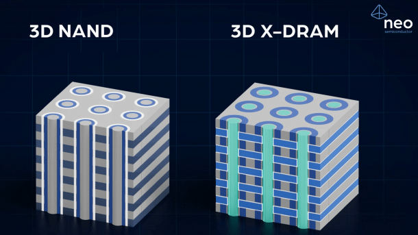
Neo Semiconductor has developed "3D X-DRAM", whose structure is similar to 3D NAND flash.
(Image: Neo Semiconductor)
In NAND flash memory, chips with several internal functional layers - so-called 3D NAND flash - have been common for years; the most complex designs have more than 200 layers. However, dynamic RAM (DRAM) for the main memory of PCs, smartphones and servers still has a "planar" structure – the individual memory cells lie next to each other, not on top of each other. This is set to change by 2030 if the roadmaps of memory manufacturers and their partners come true.
In order to increase the storage capacity of a single chip, developers will have to pack more cells onto it - with a similar silicon surface area, so that production costs remain within reasonable limits. A typical DRAM memory cell consists of a transistor (T) and a storage capacitor (C); these are also referred to as 1T1C cells.
34,359,738,368 bits to date
DRAM manufacturers currently produce individual chips with a maximum of 32 gigabits, i.e. with 34.36 billion usable cells (235= 34,359,738,368). However, these are not yet readily available, unlike 24 GBit chips for DIMMs with 24 and 48 GBytes. The next DRAM capacity steps are 64 and 128 gigabits per chip, possibly with intermediate stages of 48 and 96 GBit.

(Image: Neo Semiconductor)
A little 3D has long been a feature of DRAM: the memory capacitors of the 1T1C cells are arranged above or below the transistors to save space. Further downsizing of the individual cells is becoming increasingly difficult for numerous reasons. For this reason, DRAM manufacturers have been researching methods for several years to produce DRAM dies with several functional layers, similar to 3D NAND flash.
This does not involve several DRAM dies that are ground thin after production and stacked on top of each other, as is the case with high-bandwidth memory (HBM) or in multi-chip packages (MCPs). Instead, with 3D DRAM, there are several layers on top of each other on the same (monolithic) die. Independently of this, several (thinned) dies can be stacked on top of each other or complete wafers can be coupled to achieve even higher capacities in a memory module.

(Image: Neo Semiconductor)
The Californian company Neo Semicondutor presented its concept for 3D X-DRAM in 2023, which is designed similarly to 3D NAND flash. However, Neo Semi dispenses with conventional storage capacitors within the chip and instead relies on a floating body cell as an electron memory. With 230 layers, 128 gigabits of capacity should be possible.
For comparison: 3D NAND flash with 232 layers and triple level cells (TLC) already stores 1 terabit per die because flash cells can be packed more compactly and tightly. Production of 3D NAND with more than 300 layers is currently underway.
Samsung developers presented a paper on Vertically Stacked DRAM (VS-DRAM) at the 2023 IEEE Symposium on VLSI Technology and Circuits. Samsung is also investigating the suitability of Vertical Channel Transistors (VCT) for 3D DRAM.
Empfohlener redaktioneller Inhalt
Mit Ihrer Zustimmung wird hier ein externer Preisvergleich (heise Preisvergleich) geladen.
Ich bin damit einverstanden, dass mir externe Inhalte angezeigt werden. Damit können personenbezogene Daten an Drittplattformen (heise Preisvergleich) übermittelt werden. Mehr dazu in unserer Datenschutzerklärung.


(ciw)
