

AMD Ryzen AI 300: Surprising details about Zen 5 as well as RDNA 3.5 and XDNA2
AMD slims down the Zen 5 cores of the Ryzen AI-300 in AVX512, but the integrated RDNA 3.5 graphics have been significantly revised, as has the XDNA2 AI unit.
(Image: c't / chh)
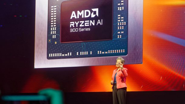
At an event for journalists and analysts in Los Angeles, California, AMD revealed further details about the Ryzen AI 300 notebook processors announced at Computex and the technology they contain.
The key data of the two new CPUs Ryzen AI 9 HX 370 and Ryzen AI 9 365 have been known since Computex, but have now been backed up with further details.
At the Techday, AMD also showed some Copilot+ notebooks from Acer, Asus, HP and MSI with Ryzen AI 300 processors that had already been announced at Computex. In several demo applications, the AI units in particular - now finally also visible as NPUs with a workload display in the task manager - showed what they were capable of. In addition to AI tools from notebook manufacturers such as Asus' StoryCube, Acer's Live Art, MSI's LMStudio and HP's AI Companion, the image generator Stable Diffusion XL Turbo and Topaz Labs' AI supporter Detail Rescuer and upscaler Gigapixel 7 were also on display. An interesting detail: None of the gaming notebooks with dGPU were equipped with Radeon Mobile.
Videos by heise
Zen 5: Core combination
AMD already developed two different core versions of Zen in the previous generation (Zen 4 + Zen 4c), which, unlike Intel's performance and efficiency cores, have the same instruction set and can therefore be controlled uniformly.
These were first used in the Epyc 9704 ("Bergamo") server processors and are significantly more compact than the originals - hence the names "Compact" and "Classic" cores. Technically speaking, the Compact cores are optimized for a different operating range on the voltage-frequency curve, the interaction of which also results in efficiency. As the operating voltage is squared in the power dissipation, it can almost always be assumed that a lower voltage leads to more energy savings than the loss in performance, i.e. the circuits work more efficiently. If you no longer need to optimize for the very highest frequencies, you can also save elsewhere and so the compact cores also occupy significantly less space than the classic versions.
The division is now also available for end users in the Ryzen 8000G, for example in the 8500G, where the Zen 4c processors only manage 3.7 GHz instead of 5 GHz in Turbo, making them around a quarter slower. In its monolothic chip, two Classic cores with a higher clock rate and four small Compact cores are combined for better response behavior.
AMD combines the Zen 5 cores in the Ryzen AI 300 similarly: four of the thick Zen 5 cores together with an eight-pack of compact cores provide the desired computing power. However, only the top model Ryzen AI 9 HX 370 gets the full twelve cores; the Ryzen AI 9 365 (without the HX top model add-on) has to make do with a 2+8 configuration. However, AMD did not specify the clock rates of the compact cores in the 300 CPUs, which manage with 28 watts as standard and can be configured between 15 and 54 watts.
The improvements to the Zen 5 microarchitecture largely apply to both core variants – except AVX512, as explained below.
AMD has significantly redesigned the front end as well as the execution units and the cache connection. Instead of one, two independent decoders now process four instructions in parallel – each with its own micro-op cache, which holds 6000 already decoded instructions. The L1 data cache grows by 50 percent to 48 KByte (12-fold associative) without reducing latency. The data path from the L1 cache to the vector unit has also been doubled – the L1 instruction cache now has two 32-bit read ports, the L1 data cache is connected with 64 bits and can fill four read operations and two write operations. All of this, as well as the doubling of the floating-point registers, is done to adequately utilize the full-speed AVX512 units. As always, the jump predictions are also improved and the out-of-order windows are enlarged. This means that more instructions can be processed and held in parallel.

(Image: AMD)
Further details will be published in an upcoming issue of c't.
AVX512 with full throughput – theoretically
As with Zen 4, the AVX512 instruction set extension is also back on board. Unlike Zen 4, the Zen 5 cores can theoretically execute AVX512 in one pass instead of two, thus ensuring twice the computing power per clock. However, AMD has also retained the option of processing the wide instructions in two 256-bit chunks one after the other to save space and energy, as Zen 4 already did.
And this is precisely what is used in both Ryzen AI 300 chips, as the "Godfather of Ryzen", AMD Ryzen chief developer Mike Clark, confirmed in an interview with c't when asked. We were interested in how AMD would handle the split between the Classic and Compact cores when the corresponding instructions were received: After all, the four thick Zen 5 cores would have just as much AVX512 performance as the eight compact versions, even at the same clock rate.
However, as it turned out, this was not a problem faced by the Ryzen AI 300 because the Classic cores in the Ryzen AI 300 work with the energy-saving option of processing AVX512 operations in two consecutive passes. However, AMD did not want to reveal whether the Classic cores use a different physical exposure mask or whether the full-speed AVX512 option is only activated via BIOS or a blown fuse.
Likewise, they did not want to reveal anything specific about the space savings of the Zen 5 Compact cores.
However, the fast AVX512 option is to be used for the Ryzen 9000 desktop CPUs, as AMD boss Lisa Su assured in her Computex speech.
RDNA 3.5: Optimized for notebooks
According to AMD, it has adapted the integrated graphics of the Ryzen AI 300 for use in the energy-sensitive notebook sector based on its licensing experience with Samsung.
Three of the most important changes are the doubling of the texture sampler, integer and compare throughput. In addition, the memory subsystem has been improved by reducing accesses through better buffering, among other things.
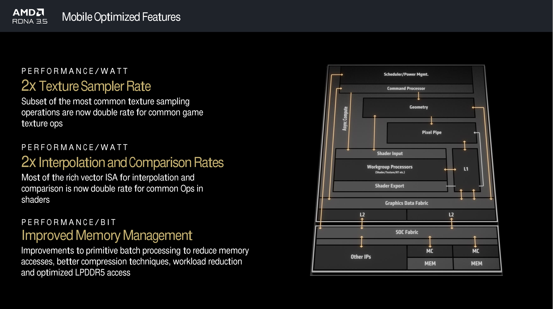
(Image: AMD)
The texture samplers are effectively data paths into the shader units, which could also be used for other calculations, for example for ray tracing graphics effects, which block parts of the texture units at AMD. These could then possibly work in parallel. The doubled integer and compare throughput in the vector units primarily leaves more time for other computing operations, as the accelerated functions are often used for preparatory tasks – Nvidia had implemented a similar change in its GeForce RTX 2000 "Turing" series.
With a power consumption of 15 watts, the Ryzen AI 9 HX 370 is said to achieve a performance of 2462 points in the DirectX 12 benchmark 3DMark Time Spy, which is around a third higher than in a similarly configured Ryzen 7 8840U.
XDNA2: AI unit upgraded
Like its predecessor, the new AI unit comes from AMD's acquired FPGA division Xilinx, specifically the Versal product line. AMD has tripled its performance compared to the Ryzen 8040 and now achieves a theoretical throughput of 50 trillion operations per second (50 TOPS) with integer precision and only slightly less when using the newly supported block FP16 format. With this, AMD aims to process the inferencing on the XDNA units of AI models already available in FP16 precision twice as fast with approximately the same accuracy. This should be possible by using a common exponent for blocks of mantissa AI models with approximately the same accuracy without additional, time-consuming quantization. A tool for the translation into block FP16 will be provided.

(Image: AMD)
The XDNA2 unit has eight groups of four execution units each, which can be individually assigned to AI applications. For many AI applications, such as the simultaneous translation of a speaker or a video filter, it is sufficient if they are executed in real time; higher performance does not benefit the user, but only costs more power. The XDNA2 unit can therefore assign the aforementioned execution units to an application in groups of five, plus a memory unit. If there is nothing else to do, the remaining unused units go to sleep.
Together with other improvements, the new XDNA2 unit should therefore work around twice as energy-efficiently as its predecessor, the Ryzen 7040.
Empfohlener redaktioneller Inhalt
Mit Ihrer Zustimmung wird hier ein externer Preisvergleich (heise Preisvergleich) geladen.
Ich bin damit einverstanden, dass mir externe Inhalte angezeigt werden. Damit können personenbezogene Daten an Drittplattformen (heise Preisvergleich) übermittelt werden. Mehr dazu in unserer Datenschutzerklärung.


(csp)
