

Switch 2: Nintendo and Nvidia rely on old 8-nanometer process
An analysis of the Switch 2 processor confirms many rumors. There is now also clarity regarding Samsung's manufacturing process.
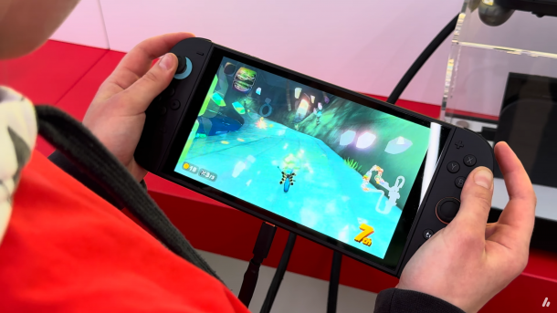
(Image: heise online)
A month before the market launch of the Switch 2, the YouTube channel "Geekerwan" has already dissected and analyzed Nintendo's console. The look at the polished processor from Nvidia is particularly exciting, confirming previous rumors and narrowing down speculation.
The name T239 is etched on the chip. It is the little brother of the T234 alias Orin for vehicles and robots. The chip structures reveal eight CPU cores. The structure is similar to Orin's Cortex-A78AE, so the assumptions about eight Cortex-A78C with ARM architecture should be correct. The AE version differs primarily in terms of certifications for use in cars.
In addition, a total of six so-called Texture Processor Clusters (TPCs), each with two shader multiprocessors, can be seen. This results in the expected 1536 shader cores. Two LPDDR5X memory modules for a total of 12 GB RAM on 128 data lines accompany the processor. The memory chips are approved for 4267 MHz (LPDDR5X-8533), but are expected to operate at a lower clock frequency in the Switch 2.
Empfohlener redaktioneller Inhalt
Mit Ihrer Zustimmung wird hier ein externes YouTube-Video (Google Ireland Limited) geladen.
Ich bin damit einverstanden, dass mir externe Inhalte angezeigt werden. Damit können personenbezogene Daten an Drittplattformen (Google Ireland Limited) übermittelt werden. Mehr dazu in unserer Datenschutzerklärung.
Old technology
Up to now, there has been disagreement about the manufacturing process. Now it is actually supposed to be Samsung's 8-nanometer process technology, which in turn is only a slight improvement on the 10 nm class. This is supported by the distances between the transistor structures, which were determined using a focused ion beam system.
They match the structures on the GA107 GPU, which Samsung also manufactured for Nvidia using 8 nm technology. This includes a so-called fin pitch of 42 nm. This refers to the distance between the transistor fins through which the current flows for switching (the process names such as 8 nm have nothing in common with the actual sizes). In newer processes, the structures would be finer.
Empfohlener redaktioneller Inhalt
Mit Ihrer Zustimmung wird hier ein externes YouTube-Video (Google Ireland Limited) geladen.
Ich bin damit einverstanden, dass mir externe Inhalte angezeigt werden. Damit können personenbezogene Daten an Drittplattformen (Google Ireland Limited) übermittelt werden. Mehr dazu in unserer Datenschutzerklärung.
The GA107 GPU belongs to the Ampere generation and is used in the GeForce RTX 3050 6 GB, among others. The Switch 2 processor uses the same Ampere architecture and is therefore at the GPU technology level of 2020. Samsung's production technology is even older – as of 2017/2018.
The old technology primarily affects efficiency compared to more modern process generations, especially from the global market leader TSMC. This in turn shortens battery life and increases waste heat – both points are a shame, especially for handheld consoles. On the other hand, the processor should be favorable for Nintendo.
Empfohlener redaktioneller Inhalt
Mit Ihrer Zustimmung wird hier ein externer Preisvergleich (heise Preisvergleich) geladen.
Ich bin damit einverstanden, dass mir externe Inhalte angezeigt werden. Damit können personenbezogene Daten an Drittplattformen (heise Preisvergleich) übermittelt werden. Mehr dazu in unserer Datenschutzerklärung.
| Vergleich Switch 2 und Switch OLED | ||
| Konsole | Nintendo Switch 2 | Nintendo Switch OLED |
| System-on-Chip | ||
| Designer | Nvidia | Nvidia |
| Fertigung | Samsung 8 nm | TSMC 16 nm |
| Prozessor | ||
| Kernarchitektur | ARM Cortex-A78C (ARMv8)* | ARM Cortex-A57 (ARMv8) |
| CPU-Kerne / Threads | 8 / 8* | 4 / 4 |
| Taktfrequenz | unbekannt | 1,02 GHz |
| Grafikeinheit | ||
| GPU-Architektur | Nvidia Ampere* | Nvidia Maxwell |
| Shader-Multiprozessoren | 12 (1536 Shader-Kerne)* | 2 (256 Shader-Kerne) |
| Taktfrequenz | 561-1000 MHz* | 307-768 MHz |
| FP32-Rechenleistung | max. 3,1 TFlops* | max. 0,4 TFlops |
| Speicher | ||
| Menge, RAM-Typ | 12 GByte LPDDR5-6400 oder -7500* | 4 GByte LPDDR4-1600 |
| Übertragungsrate | 102,4 oder 120 GByte/s* | 25,6 GByte/s |
| Display | ||
| Größe | 7,9 Zoll Touch | 7 Zoll Touch |
| Auflösung | 1920 × 1080 | 1280 × 720 |
| Bildwiederholrate | 120 Hertz mit VRR-Support | 60 Hertz |
| Paneltyp | LCD (IPS) | OLED |
| Massenspeicher | ||
| Kapazität | 256 GByte | 64 GByte |
| Speichertyp | UFS | eMMC |
| Erweiterung | microSD Express | microSD UHS-I |
| Anschlüsse | ||
| Audio | 3,5-mm-Klinke | 3,5-mm-Klinke |
| USB | 2x Typ C (Geschwindigkeit unbekannt) | 3.2 Gen 1 (5 Gbit/s) Typ C |
| Sonstiges | ||
| Gewicht | 401 / 534 g (ohne / mit Joy-Con) | 320 / 420 g (ohne / mit Joy-Con) |
| Größe | 272 mm × 166 mm × 13,9-30,7 mm | 242 mm × 102 mm × 13,9-28,4 mm |
| Preis | 470 Euro (UVP) | 360 Euro (UVP), ab 290 Euro verfügbar |
| *nicht von Nintendo bestätigt | ||


(mma)
