

Samsung flash: Allegedly 400 memory layers with hybrid bonding
The technology used by AMD for the Ryzen X3D is apparently also to be used by Samsung for SSD memory, based on YMTC.
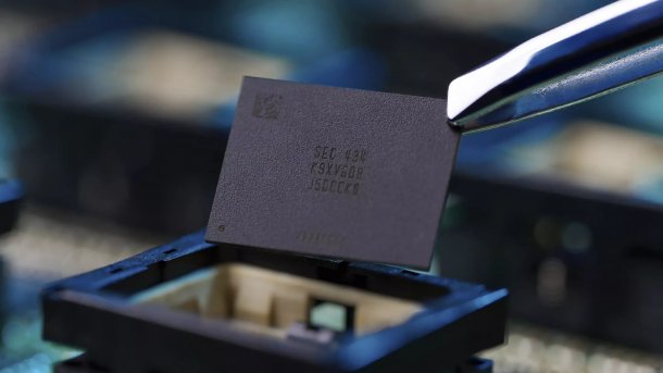
Samsung's V-NAND V9, which is still monolithic.
(Image: Samsung)
Samsung apparently wants to produce NAND flash components with at least 400 memory layers, called V-NAND V10 by the manufacturer, from 2026. These chips are intended to further increase the capacity of SSDs. Samsung itself has not disclosed the number of layers of its memory for some time – According to analyses, the V9 generation stands at 286.
Samsung and most other major NAND flash manufacturers have so far exposed all memory structures on a single wafer: the logic for controlling the memory is located on the base level, with the memory cells located above it. Etched through-silicon vias (TSVs) connect all layers with each other.
Chip separation
Samsung is reportedly taking a new approach with the 10th generation: The logic part and the memory layers are to be exposed separately on different wafers. The chips are then joined together to form a memory module using a process known as hybrid bonding. Hybrid bonding works without solder joints: The silicon is ground flat and precisely stacked so that the contact tips and surfaces adhere to each other sufficiently strongly. AMD and its chip contract manufacturer TSMC have been using this technology for years in the Ryzen X3D processors with stacked cache.
Videos by heise
The Korea Economic Daily (KED Global) reports on the 400 memory layers, while the analysis company Techinsights also reports on hybrid bonding.
Most major memory manufacturers have so far built their NAND flash monolithically. Chinese manufacturer YMTC, which calls the technology Xtacking, has already split it in two. The procedure is intended to enable more memory layers, but also increases production costs.
Other manufacturers will also increase the number of memory layers in the coming years. SK Hynix, the second largest manufacturer after Samsung, will take an intermediate step with 321 layers in 2025.
Empfohlener redaktioneller Inhalt
Mit Ihrer Zustimmung wird hier ein externer Preisvergleich (heise Preisvergleich) geladen.
Ich bin damit einverstanden, dass mir externe Inhalte angezeigt werden. Damit können personenbezogene Daten an Drittplattformen (heise Preisvergleich) übermittelt werden. Mehr dazu in unserer Datenschutzerklärung.


(mma)
