

HBF: 4 TByte memory on one GPU
Sandisk wants to pack an extremely large amount of fast flash memory onto GPU accelerators. Large language models would thus fit on a GPU.
(Image: Sandisk)
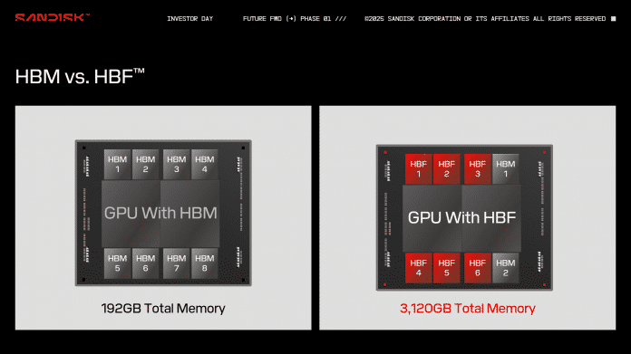
High-bandwidth memory (HBM) has competition. The NAND flash manufacturer Sandisk is proposing the memory form High-Bandwidth Flash (HBF) for AI accelerators. Instead of DRAM chips (Dynamic Random Access Memory), the eponymous NAND flash is used, which is optimized for many parallel accesses.
The advantage of flash is that it achieves significantly higher storage capacities than DRAM on the same surface area. An HBF module is said to hold 512 GB – 21 times more than the current HBM3e generation. The latter currently has 24 GByte; 48 GByte will follow next. HBF should enable 8 to 16 times as much capacity at similar costs. Conversely, Sandisk is therefore calculating with higher costs per HBF module.
HBF uses the same memory interface as HBM. Each module is therefore connected to the GPU via 1024 data lines. However, due to necessary protocol changes, the flash alternative cannot be exchanged one-to-one for HBM. With this connection, the technology is not comparable with earlier attempts to place SSDs on a graphics card and connect them via PCI Express.
4 TByte memory on current GPUs
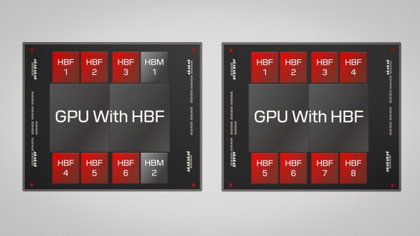
In a presentation, Sandisk's future Vice President for Memory Technology Alper Ilkbahar references Nvidia's Blackwell GPUs B100 and B200. Eight HBF devices would result in 4 TByte of memory (4096 GByte). The engineer emphasizes that this is enough for large modern AI language models on a single GPU. GPT4, for example, would take up around 3.6 TByte with 1.8 trillion parameters.
Alternatively, manufacturers could mix HBM and HBF. Sandisk previously planned a combination of six HBF (3072 GByte) with two HBM modules (48 GByte). The DRAM could then contain data such as for the key-value cache (KV cache) of AI models, which is continuously written.
Sandisk High-Bandwidth Flash (HBF) (4 Bilder)
Sandisk
)However, Ilkbahar now cites innovations such as DeepSeek's Multi-Head Latent Attention (MLA) cache technology, which shrinks the space requirement of the KV cache to a fraction and requires fewer write instructions. DRAM could thus become superfluous for AI training.
High read performance with 16 memory layers
HBF would be particularly fast for read accesses. Sandisk speaks roughly of the same transfer rate as with HBM. Eight components together should therefore be able to transfer several terabytes per second, at least in read mode. Sandisk is silent on the write speed.
For the high read speed, Sandisk divides each NAND flash chip into countless memory areas, which are addressed in parallel by a controller. In an HBF device, 16 NAND flash chips (“16-Hi”) are located on a logic layer for the controller. As with HBM, a silicon interposer establishes the connection with a GPU. Alternatively, manufacturers could stack HBF on a GPU. It could also be used with CPUs or other processor types.

(Image: Sandisk)
Like HBM, HBF is to become an open standard, meaning that other manufacturers could also produce it in the future. Development is said to have started in 2024 with proposals from “important AI players” – so there already seems to be interest in the industry. Sandisk is not specifying when high-bandwidth flash will be ready for the market.
Meanwhile, HBF is not an option for gaming graphics cards. Even with HBM, the costs for graphics cards are considered too high. In addition, games benefit from low access latencies, which are better with DRAM than with flash.
Empfohlener redaktioneller Inhalt
Mit Ihrer Zustimmung wird hier ein externer Preisvergleich (heise Preisvergleich) geladen.
Ich bin damit einverstanden, dass mir externe Inhalte angezeigt werden. Damit können personenbezogene Daten an Drittplattformen (heise Preisvergleich) übermittelt werden. Mehr dazu in unserer Datenschutzerklärung.


(mma)
